XFX nForce 780i SLI | bit-tech.net
Manufacturer:XFX
UK Price (as Reviewed):£156.55
US Price (as Reviewed):$241.52
Introduction
We took a quick glance at the new nForce 780i SLI chipset motherboard just before Christmas in our first look. Since, we’ve confirmed that only XFX will offer the reference design in the UK and Europe, with EVGA covering the United States.
There are less partners involved in the reference design this time around, unlike with the nForce 680i SLI which had half a dozen typically graphics companies joining the motherboard fold to sell the same board. Instead, we have a far greater differentiation from a range of Tier 1 motherboard manufacturers like Asus, Gigabyte, MSI and Foxconn with nForce 780i SLI.
We’ve also heard more about the NF200 chip that permeates the new nForce 700-range — instead of just being just a splitter chip for PCI-Express 2. 0 there’s actually some clever engineering in that little bit of silicon, predominantly concerning SLI. Apparently when the nForce 700-series launched there were certain patents pending, so Nvidia couldn’t talk about it in the depth it would have liked.
These new features include a Posted Write Shortcut, which allows data from one graphics card to be passed directly to other cards without having to navigate back to the CPU, reducing the need for several stops and a lot more latency to the journey. This should particularly help in simple two-card SLI setups, which are now controlled entirely by the NF200 chipset, however it won’t help in the new 3-way love-fest as much.
Click for larger images
There’s also a CPU Broadcast function that iterates commands from the CPU to multiple graphics cards connected to the nForce 200 in a single turn, again reducing command latency. The NF200 chip is connected to the chipset with just a single PCI-Express 2. 0 link, but it should still be more than enough considering graphics cards don’t even fill a normal 1.1 link. That said, it does kind of invalidate the half the reason of upgrading to PCI-Express 2.0. Both the NF200 features are designed to reduce traffic between the chipsets as well as reduce command latency.
Does any of this make a real difference though? Or is the nForce 780i SLI just simply too much of an nForce 680i SLI clone?
Nvidia ESA
Currently out in beta here, Nvidia system tools have been updated to include ESA support for Nvidia 700-series motherboards. If you’re unfamiliar with ESA, or Enthusiast Systems Architecture, then check out our preview for more information.
There are a few parts to the Nvidia software; for starters there’s the System Monitor which is the main hub and does exactly what it says on the tin. Loading it up presents you with a 3D interface of all the components spinning around a central axis, revealing their status. It’s very elaborate, excessively so, but it makes for something good to show off at least. At first there’s the inevitable «Wow, this is cool», only to realise that it lacks actual usability since it takes up your entire screen and looking at each, individual component separately is labour intensive and inefficient.
What it does do right is potentially tie in your whole system to a hub — providing you invest in an ESA case, PSU, watercooling kit or air cooling heatsink, Nvidia graphics card and EPP memory to get the full effect. Are you really prepared to buy everything again, and restrict your purchasing decision to buy certain ESA kit? There are certainly pro’s and con’s to the entire equation.
The software also offers an event logging function so you can monitor selected parts in the background, and thankfully it still has an updated set of desktop graphs that provides far better usability. There’s component name customisation so you can differentiate between parts – like two identical hard drives for example, and generally everything is there on your desktop at a glance. Unfortunately this currently doesn’t work too well — it should just switch by clicking the arrow in the top right, but that simply minimises the 3D instead. Ideally there would be a Vista Sidebar option too, for those of us that want to streamline it into our other desktop applications.
The control panel is certainly very good — it’s not held back by Taiwanese «design» (I use the word loosely in terms of motherboard software) and is very easy to navigate, like all Nvidia software previously has been — task list drop down on the left, device settings on the right.
Currently it’s still very beta though — the reported status of many system functions was clearly wrong and some parts just simply don’t work at all. ESA is still a very young initiative, but with the likes of hybrid SLI and further core hardware features arriving in the next six months, it might become a platform worth investing in.
Flip the page and we’ll get on with the testing of this fine piece of kit. ..
..
1 — XFX nForce 780i SLI2 — Test Setup3 — Subsystem Testing: Memory and Drive Performance4 — Subsystem Testing: Audio Performance5 — Real World Test Results6 — Gaming Performance and Power Consumption7 — Rounding up and Final Thoughts
XFX nForce 780i SLI Motherboard Review
By Nathan Kirsch •
NVIDIA Updates The 680i SLI With a Bridge Chip!
NVIDIA has had PCI Express 2.0 compliant video cards out on the market for a month now, but didn’t offer a platform that supported this new feature. NVIDIA also didn’t have an Intel platform that could power the latest Intel 45nm Quad-Core Yorkfield processors. When it comes to selling chipsets and motherboards you have to support the latest and greatest technologies and it was obvious that NVIDIA was falling behind.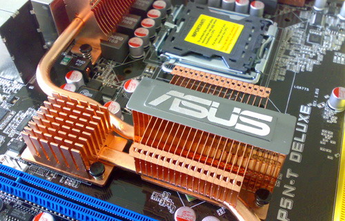 NVIDIA originally claimed the 680i SLI chipset would support all 45nm dual-core and quad-core processors, but that came to an end when Intel made some changes on their latest stepping on their 45nm quad-core Yorkfield processors. It’s tough to promise support for something more than a year away and it’s obvious that NVIDIA said a little too much too soon. The 680i SLI motherboard series came out on November 8th, 2006 and has been in need of an update, so the 780i SLI chipset is a welcomed addition to the market.
The 680i SLI and 780i SLI motherboards are undoubtedly similar, but they do have some distinct differences. The NVIDIA 780i brings the following changes:
-
Native Yorkfield and Wolfdale support
-
PCI-Express 2.0 certification
-
3-Way SLI support (3 full x16 lanes)
-
Optimized for new software including new NVIDIA Control Panel and NVIDIA System Monitor
-
Refined BIOS for overclocking (ie: ability to use half multipliers, etc.
 )
)
Basically what NVIDIA has done is some tinkering on the motherboard in order to support 45-nm quad-core processors, but that was strictly done on the board level and not in the chipset. The 680i SLI series will support 45nm dual-core processors as is, but they will not post with 45nm processors as we found out here. Since the change is on the motherboard there is nothing holding back motherboard makers from coming out with a newly revised 680i SLI motherboard to support 45nm quad-core processors. Legit Reviews recently spoke with eVGA about this and they informed us that eVGA has no plans for a new revision. This makes sense as it would hurt their 780i SLI motherboard sales.
NVIDIA has refined their BIOS for overclocking as they have added half multipliers to the mix, which allows you to better dial in your overclock. They have also some newer software revisions for NVIDIA control panel and system monitor. The new hardware features include 3-way SLI support with 3 full x16 lanes, which is great for those that have $1500+ to spend on three GeForce 8800 GTX or Ultra graphics cards. An NVIDIA nForce 200 chipset is used to help give the board it’s 3 full x16 lanes of which two are PCI Express 2.0 ready. Why are just two PCI Express 2.0 compliant?
To improve the time to market for this motherboard series, NVIDIA opted to use an NVIDIA nForce 200 chipset to add the new features of the board. Traditional motherboards have two chipsets on them: a north bridge, which Nvidia calls a System Platform Processor (SPP), and the south bridge, which Nvidia calls the Media Communications Processor (MCP). The NVIDIA 780i motherboard has a third chipset on it now, which is the nForce 200. The nForce 200 connects directly to the north bridge and adds 32 lanes of PCIe 2.0 connectivity that can be split evenly between a pair of physical x16 slots. There are not enough lanes for three physical x16 PCI Express 2.0 slots, so the thrid lane goes directly through the nForce 780i SLI MCP. Of the 62 PCIe lanes, 32 are PCI Express 2.0 and they are all thanks to the nForce 200 chipset. This isn’t the best way to implement 3-way SLI support, but it works.
Why is it not the best way? According to PCI-SIG, the PCI Express Base 2.0 specification doubles the interconnect bit rate from 2.5 GT/s to 5 GT/s in a seamless and compatible manner. The performance boost to 5 GT/s is by far the most important feature of the PCI Express 2.0 specifications. It effectively increases the aggregate bandwidth of a 16-lane link to approximately 16 GB/s. The interface between the NVIDIA nForce 780i SLI SPP and the NVIDIA nForce 200 provides maximum bandwidth of 4.5 GT/s per link, which is below the 5 GT/s that is stated in the PCI Express 2.0 specifications. This gives the 780i SLI platform an aggregate bandwidth of a single 16-lane link to be 14.4 GB/s, which is just under what the 16 GB/s total bandwidth that a PCIe 2.0 slot should have in an ideal world. What NVIDIA has done with the 780i SLI is ‘good enough’ for today’s PCI Express 2.0 graphics cards, but what about the future? The image above shows the nForce 200 chip next to the larger north bridge or System Platform Processor (SPP).
Questions or comments?
View this thread in our forums!
nForce 780i SLI – a cosmetic update of the
superplatform
Since the release of nForce 680i SLI, the question of what is considered a top chipset for Intel processors has become much more complicated. One of Intel’s own products always had this status, but on the third try, NVIDIA turned out such a successful set of system logic and a reference motherboard design that the throne under the Intel 975X shook. However, for 2007 Intel released a new flagship chipset called X38 and is preparing to launch X48. We had to wait a long time for NVIDIA’s answer, and it turned out to be not quite «symmetrical». It will be all the more interesting to compare the novelty with the hi-end class solutions already established on the market. nine0003
Help
The NVIDIA nForce 7x0i series for Intel processors is a new family of chips designed to support next-generation products and technologies — 45nm CPUs, PCI Express 2. 0, 3x SLI, ESA, and more.
As with the last generation of chipsets, the first to enter the market is the top variant, i.e. nForce 780i SLI, and it is in the form of a copy of the reference design of the NVIDIA motherboard under the EVGA and XFX brands. Officially, these boards were supposed to appear at the end of 2007 (since the chipset was announced on December 17), but in practice, even at the end of January, they are available on our market in very small quantities and only in the EVGA version. Also in December, the ASUS P5N-T Deluxe board based on the original PCB was supposed to be released, but so far it has not reached our Test Lab. Two more models based on the same chipset, made according to their own designs, are announced for release in January: Gigabyte GA-780ISLI-DS5 and MSI P7N Diamond. nine0003
As for the entry-level nForce 750i SLI, only three motherboards have been officially confirmed to date: ASUS P5N-D, Gigabyte GA-750ISLI-DS4 and MSI P5N Platinum. None of them are on the market at the time of this writing. Naturally, other models will obviously appear on a more affordable chipset, but even later.
Course
MANAGER FOR WORK WITH CLIENTS
Become a demanded trader and withdraw your offer.
REGISTER! nine0003
ZMIST
- 1 Chipset NFORCE 780i SLI
- 2 Maternal board EVGA 132-KK-NF78-A1
- 3 Verdict
9003 configuration atypical for desktop products. The north bridge of the 780i SLI SPP (like the 680i SLI, it is manufactured by TSMC on a 90nm process) provides interfaces for the processor, RAM, two PCI Express x1 lanes, and also interacts with the MCP via the HyperTransport bus and with the nForce 200 chip responsible for the implementation PCI Express 2.0. nine0003
The chipset officially supports Intel processors in the LGA775 design with a system bus frequency up to 1333 MHz inclusive, as well as models manufactured using the 45-nanometer process technology. At the same time, NVIDIA separately notes the use of CPUs based on Yorkfield and Wolfdale cores — as you know, such a possibility was not expected for nForce 680i SLI, although ASUS has already released updated BIOSes for its boards based on this chipset. But to implement support for upcoming CPUs with a clock frequency of 1600 MHz (i.e. Intel Core 2 Extreme QX9770) NVIDIA hesitated. Although, this will probably be done later by releasing a new BIOS firmware, because there should not be any restrictions on this in the design.
As for RAM, in this part the specifications duplicate those of the previous generation: 780i SLI SPP uses only DDR2 memory (but up to DDR2-1200). Of course, compatibility with modules that have the EPP (Enhanced Performance Profiles) SPD extension, also known as «NVIDIA SLI-Ready Memory» and which has long become popular with DRAM manufacturers, has been preserved. The lack of DDR3 capability is likely to frustrate enthusiasts — back in 2007, the new standard proved its viability and excellent performance, albeit at an inflated price so far. According to unofficial data, DDR3 support will be implemented in the nForce 79 chipset0i SLI, which should be announced by NVIDIA in the coming months.
The second chip in the nForce 780i SLI is an unusual addition to the standard northbridge/southbridge layout. The chip is called NVIDIA nForce 200 (internally labeled NF200-SLI) and is a PCI Express switch with one incoming and up to four outgoing ports (with the possibility of direct interconnection between these four) with a total of 32 lanes. Frankly, right now the need for PCIe 2.0 isn’t there yet, and the benefits of the faster standard will really show up in the next generation of graphics cards at best. nine0003
The nForce 780i SLI has as many as 62 PCI Express lanes, and they are implemented by all three chips. As already mentioned, 32 lanes is PCI Express 2.0, which is what the NF200-SLI is responsible for. The third full-featured PCI-Express x16 slot on the board is provided by the southbridge, while it (like the rest of the slots listed below) belongs to the PCIe 1.0 standard, which does not interfere with assembling 3xSLI class systems. Due to the south bridge, there is one more PCIe x8 slot and four x1 slots. But the last two PCI Express 1.0 x1 can be separated on the motherboard from the northbridge chip — as if all of the above was not enough . .. Of course, there cannot be so many ports on one board, and the reference design assumes the following configuration of connectors located on the PCB: 2x PCI Express 2.0 x16, 1x PCI Express 1.0 x16 and 1x PCI Express 1.0 x1 (that is, in total, 32 out of 32 possible PCIe 2.0 lanes and 17 out of 30 PCIe 1.0 lanes are available to the user). Probably, there has never been a more ingenious topology of expansion interfaces of the same type on motherboards …
The nForce 780i SLI is currently the only Intel platform solution that supports three full-speed PCI Express x16 graphics slots. Therefore, the 780i SLI is an ideal candidate for a 3xSLI PC. However, this topic deserves a separate article with a detailed study of the real performance of such a superconfiguration — in the next issues we will return to the issue of 3×SLI.
The southbridge chip in the nForce 780i SLI chipset has not changed compared to its predecessor: it’s still the same… in fact, the northbridge of the single-chip chipset — nForce 570i (NF570I), but in this case it performs MCP functions. It is connected to the SPP via the HyperTransport bus and is responsible for the typical southbridge feature set (PCI, USB 2.0, HD Audio, SATA RAID, etc.), but it is also the first ESA-certified device. nine0003
ESA stands for Enthusiast System Architecture and is the new open, free industry standard for real-time product control and monitoring. By adopting ESA, PC builders and enthusiasts get a more customizable solution and better PC performance than is possible with proprietary solutions. Monitoring various PC parameters is a critical task for the efficient operation of the system, and ESA allows you to expand the list of devices with «feedback» to power supplies, cases and water cooling systems — i.e. components that previously did not provide any information about themselves. nine0003
ESA specifications define the information protocol by which system components communicate information about their operation and can be configured by the user. To do this, each ESA-compatible device contains the necessary sensors and a microcontroller that processes the incoming analog information from the sensors and transmits it to the motherboard via the USB bus.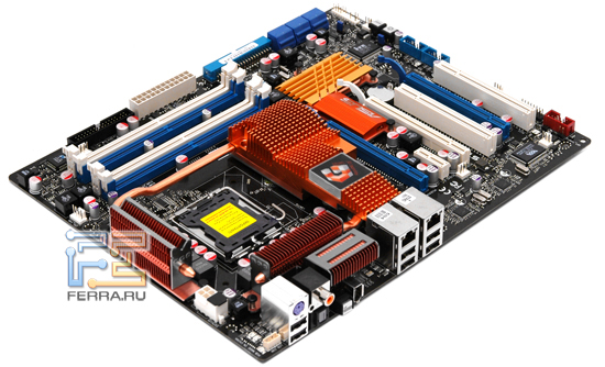 Moreover, the specific monitoring and control capabilities of the device are determined by its manufacturer, and the ESA standard is only responsible for a single data transfer mechanism. Certification of devices is entrusted to the Taiwanese test organization Allion, which checks the cross-compatibility of new equipment and its compliance with the ESA specification, after which the company receives the right to use a certain logo. To date, the ESA architecture is supported by a very small number of devices, but their list is growing — for example, Thermaltake, one of the leaders in this industry, recently announced ESA certification of several of its products. nine0003
EVGA motherboard 132-CK-NF78-A1
Comparing the board design based on the new chipset with its predecessor, it’s hard not to notice some improvements in an already excellent product. The placement of the components remained almost unchanged, but the heat pipe cooling system (the weak link of the NF 680i SLI with a high level of heat) has been substantially strengthened, and even the design has become closer to NVIDIA’s corporate colors. Some connectors have been moved, which made it easier to assemble a PC in a case. Near the connector for the processor cooler, an LED indicator of CPU overheating has appeared. In fact, there is only one remark, and that is important only for owners of 3×SLI systems: when installing three video cards of the GeForce 8800 Ultra format, not a single expansion slot is available anymore — neither PCI-Express x1, nor PCI. This creates a serious limitation on the functionality of a super-PC, because even a high-quality sound card cannot be used! Otherwise, there are no complaints about the design.
nine0003
The BIOS settings were very detailed in the previous generation of NVIDIA’s top motherboards, so there are only some additions in the form of «half» multipliers for the CPU or four separately adjustable voltages of the GTLVREF group (this feature can help with overclocking).
With the NVIDIA Control Panel, most of the key system settings can be changed through Windows without rebooting or entering BIOS Setup. The list of available real-time adjustments includes the FSB frequency, the level of supply voltages, the fan speed, etc. With an ESA-compatible PSU, chassis and cooling system, the user can also control their operation using the same software. The interface of the NVIDIA System Monitor program has been improved, which can now function in 3D mode with OpenGL rendering.
nine0003
Verdict
Comparing the EVGA 132-CK-NF78-A1 with the ECS PN2SLI2 Extreme based on the nForce 680i SLI reference design, we found that the impressive performance of the DDR2 controller in the top NVIDIA chipset was not only preserved, but even slightly increased — though quite a bit. Little. As a result, the performance in test applications of the two chipsets is almost identical with a slight advantage of the new product, and both products outperform DDR2 boards based on Intel X38 and P35. Whether there is any difference in 3D applications between these solutions — we will find out in the material on 3xSLI. The nForce 780i SLI’s FSB overclocking capabilities are quite large, and the GTLVREF voltage adjustment really allows you to «squeeze out» an extra ten megahertz of the system bus frequency.
nine0003
Considering that the NF 780i SLI is very close to its predecessor in terms of performance, functionality and behavior of the boards, the tests did not reveal any surprises. But the impression of the novelty remained extremely positive, because NVIDIA has successfully upgraded an already extremely successful chipset. So the updated flagship nForce continues to seriously compete with the flagship chipset from Intel, this time X38. And, as before, for those who want to use two video cards from NVIDIA in their PC based on an Intel processor, there are no alternatives to the NF 780i SLI.
nine0003
| Processor | Intel Core 2 Extreme X6800 (2.93 GHz, Conroe) |
| RAM | 2×Corsair Dominator CM2X1024-8888C4D (@ DDR2-800 4-4-4-12) |
| Video card | XFX GeForce 8600 GT Fatal1ty |
| Hard disk | WD Raptor 36 GB SATA |
| Power supply | PC Power & Cooling Turbocool 1KW-SR |
| Corsair | Corsair | www. corsairmemory.com corsairmemory.com |
| ECS | ECS | www.ecs.com.tw |
| EVGA | Nebesa | www.nebesa.ua |
| Intel | Intel | www.intel.com |
| PC Power & Cooling | Nebesa | www.nebesa.ua |
| XFX | XFX | www.xfxforce.com |
See also:
Detailed review on ModLabs.net
|
Computer games | Secrets for games | Games industry news | Articles about games |
|

